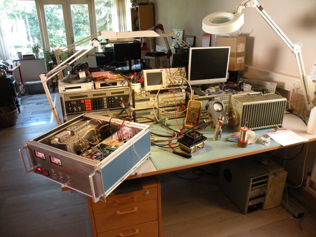
144MHz LDMOS SSPA
Project Progress
19.08.2011: Flash news: It's now officially a functional amplifier - read on below!After having worked on a 4 xMRF151G for more than three
years, but never finished it due to my inability to
devise a satisfactory combiner, I saw the LDMOS
project described in Dubus 4/2011 by F1JRD http://www.qsl.net/f1jrd/MRFE6VP61K25H.html
This would certainly solve my problem as it uses only one device for up to 1.2KW output!
I promptly decided to go this route, and bought the necessary parts
from various sources, while retaining most of what I had already built
for the previous (failed) project:
http://www.rfham.com/index.html?c85.html
I also decided to use the control and display project designed by F1TE for this project:
http://www.f1te.org/index.php?option=com_content&view=article&id=22&Itemid=48
http://www.f1te.org/index.php?option=com_content&view=article&id=25&Itemid=50
http://www.f1te.org/index.php?option=com_content&view=article&id=29&Itemid=55
A Finnish group is working on a HF + 50MHz amplifier kit based on this device: http://www.nikkemedia.fi/juma-pa1000/
One of my design goals is to be able to run full power for
extended periods of time, primarily for EME work, so first problem is
design of a sufficient cooling arrangement:
This is what I came up with:
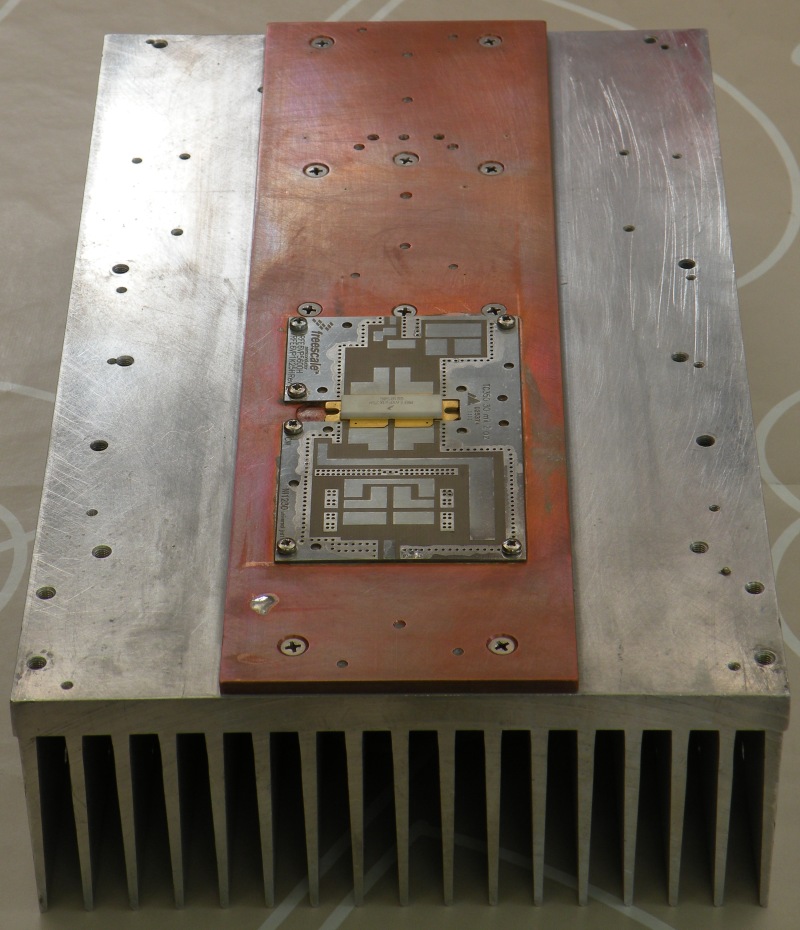
The heatsink itself is 35x20x10cm and weighs about 7Kg, with the Cu
heat-spreader (10x35x0.5cm), the whole assembly weighs about 8.5Kg! Now
it should only be a question of moving a sufficient amount of air
through the heatsink, more on that later.
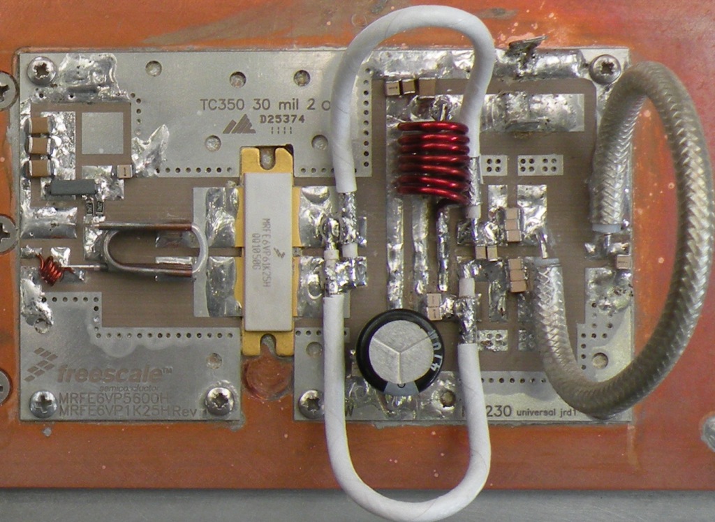
I also decided to adopt the suggestions about soldering the LDMOS
device and the PCB to the Cu Heat-spreader. This was accomplished using
solder paste and a household oven (this process smells BAD, so don't do
it while the XYL is home) it took about 1 hour with the termostat set
to 250 degrees centigrade before the solder finally melted and
completed the baking phase!
I had to bake the entire assembly, as some of the screws mating the Cu
piece to the Al one are located underneath the PCB (remember this part
of the project was fabricated prior to the adoption of the LDMOS device.
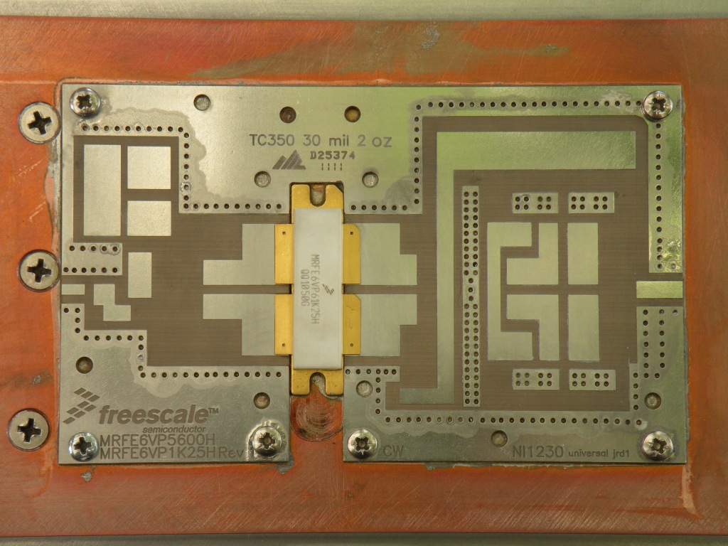
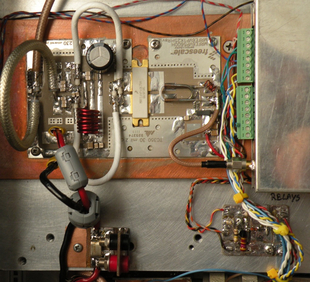
Close-up of the soldered LDMOS device and PCB.
A check with a transistor tester showed that the two separate transistors survived the baking process!
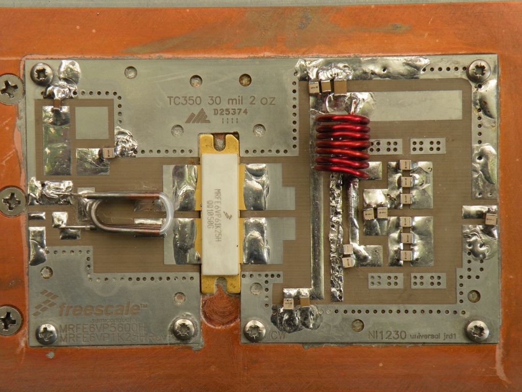
Here most components are soldered to the PCB using 5% Silver solder.
Actually soldering components onto the PCB attached this way, is a
cast iron bitch - I finally heated the whole assembly to some 150
degrees again to accomplish this, particularly the through-plated
ground pads are difficult because of the excellent heat transfer of
this assembly method (which was the goal anyway).
24.06.2011:
F1JRD, Lionel (the designer of the SSPA RF-module) found this website,
and was kind enough to let me know that he was far from happy with the
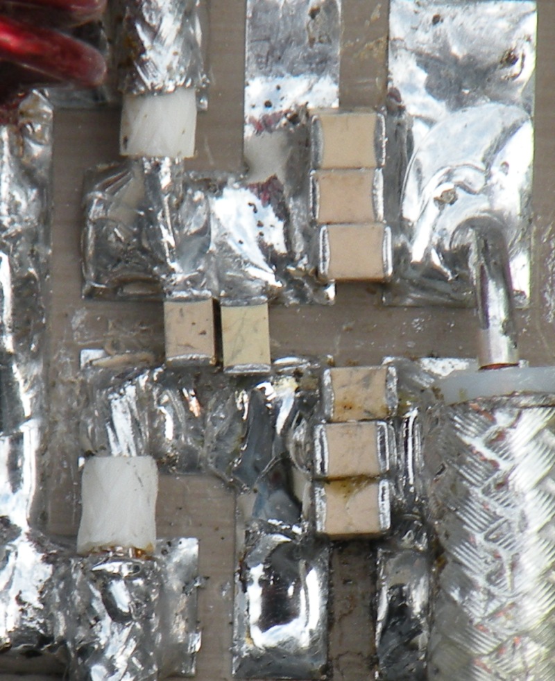
way I had mounted some of the capacitors on the board (circled in red
below):
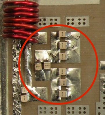
He pointed out that there was a definite risk that the spacing
between the individual caps would result in an uneven RF-current flow
through them, and that this could lead to failure of them and/or
self-oscillation. He prescribes that they be mounted on the edge and as
close together as possible, I took a chance and remounted them loosing
only one 15pF cap in the process - luckily i had a spare in my
RF-components junk box.
This i what it looks like after the remount:
The RF-module is now complete (but still untested) and I am working on the completion of the F1TE control and safety circuit.
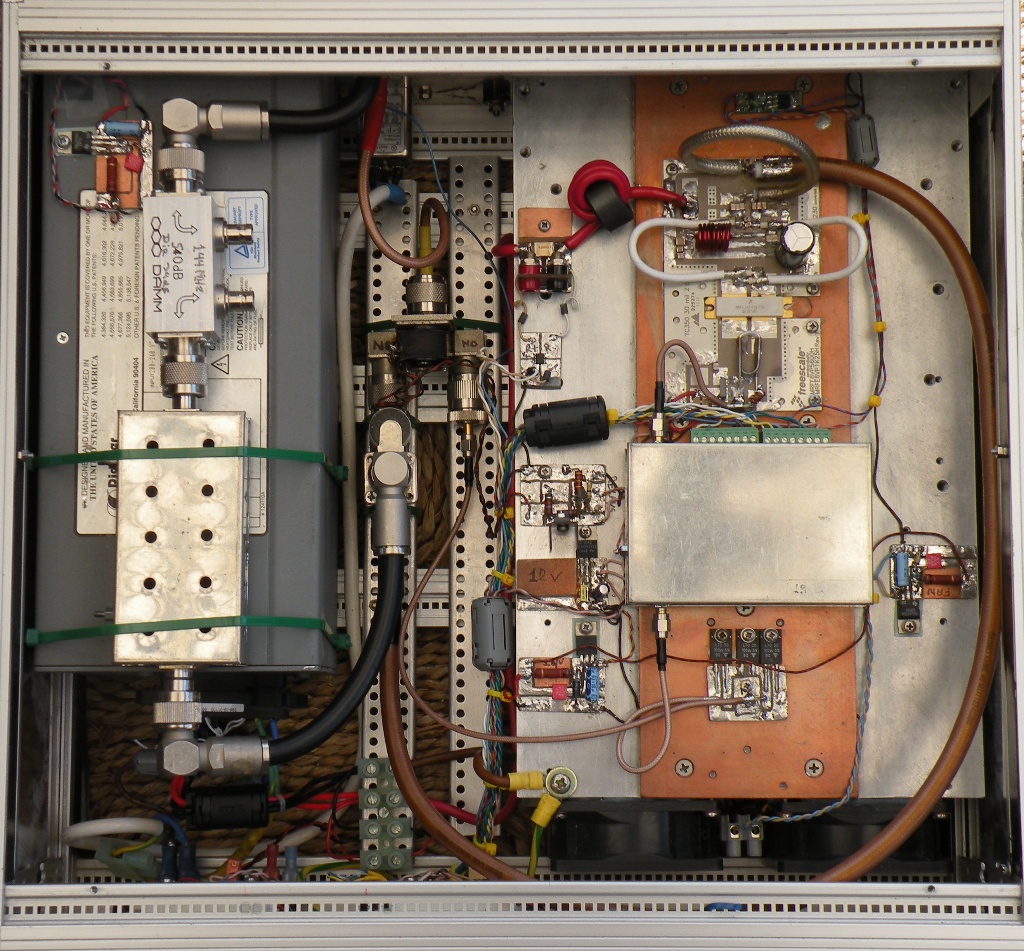
This illustrates my planned general layout of the "Business end" of the amplifier:
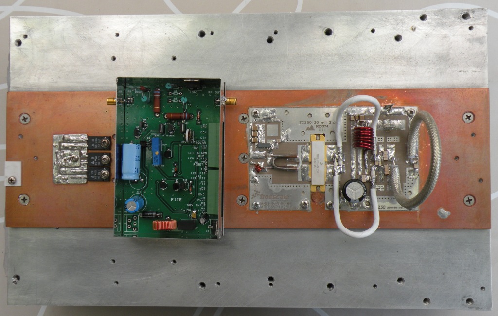
From left to right: 12dB power-attenuator (to reduce the 50W from my
FT-847 to 3W); F1TE control PCB (almost completed); and on the right
the RF-module itself. In various positions will go the temperature
sensing module (F1TE), circuits to produce 24V and 12V from the 50V
main supply (See: http://www.frenning.dk/OZ1PIF_HOMEPAGE/Various_circuits.html
and my fan-speed controller (See: http://www.frenning.dk/OZ1PIF_HOMEPAGE/Fancontrol.htm ).
09.07.2011: I'm now ready
for initial power-up testing, all the essential components are in place
and working bar one! The F1TE PWR/SWR display/alarm module (Ver. 2)
sadly does not work!, and is beyond my abilities to fix/redesign. So
for now I don't have any SWR protection, until I come up with a "plan
B".
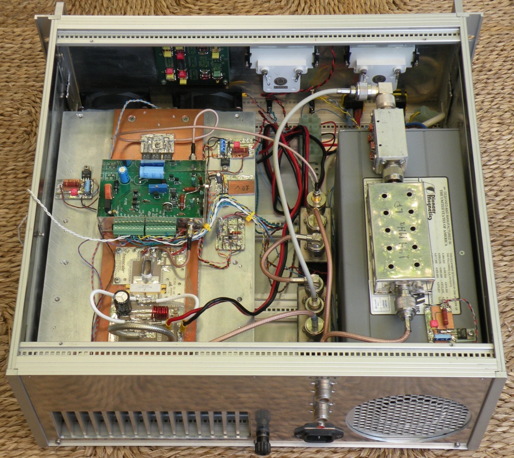
Seen from the rear: leftmost supply module for the two "hot" fans
(24V/6W, operated at ~16V for reduced noise), switched on at heatsink
temperature 45॰C by F1TE's Temperature module. The Power Supply
(Pioneer Magnetics, at right) fan runs at reduced RPMs at all times; Cu
pallet from rear to front: Temp. Module, RF-Module, F1TE Control-Module
and 12dB power-attenuator; To the right of of the Cu-pallet (from front
to rear) Voltage regulator 50V-> 26V, 7812 26V->12V (supplies
Control-Module) and finally relay driver operated by voltage taken from
R8/Q2 junction in the Control-Module. In the middle two Radiall 24V
coax relays, and on top of the power supply LP-filter and Directional
Coupler, these will probably be relocated to fit next to the relays
later. Mounted on the Front-cover are two display instruments and an
(unfinished) SWR/PWR display module.
The white twisted wire hanging over the side (with a invisble
push-button switch at the end) is for Fault-simulation during testing.
You do, of cause, use a decent LP-filter in you amplifier - don't you? I use a design, by AF9Y, Mike W. Cook, with very good rejection of 2'nd and 3'rd harmonics and miniscule insertion loss:
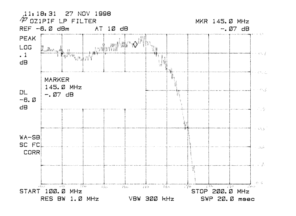
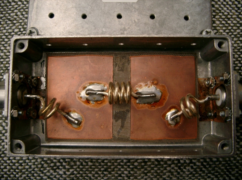
Here mounted in a slightly different box, the current iteration seen in this amplifier is built in a tinned sheet box, as seen below.
If you need information on this filter please contact me off-line, unfortunately I cannot publish it here, since AF9Y cannot be contacted for permission..
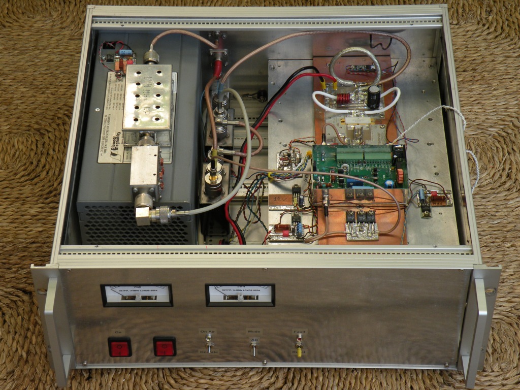
From the front...
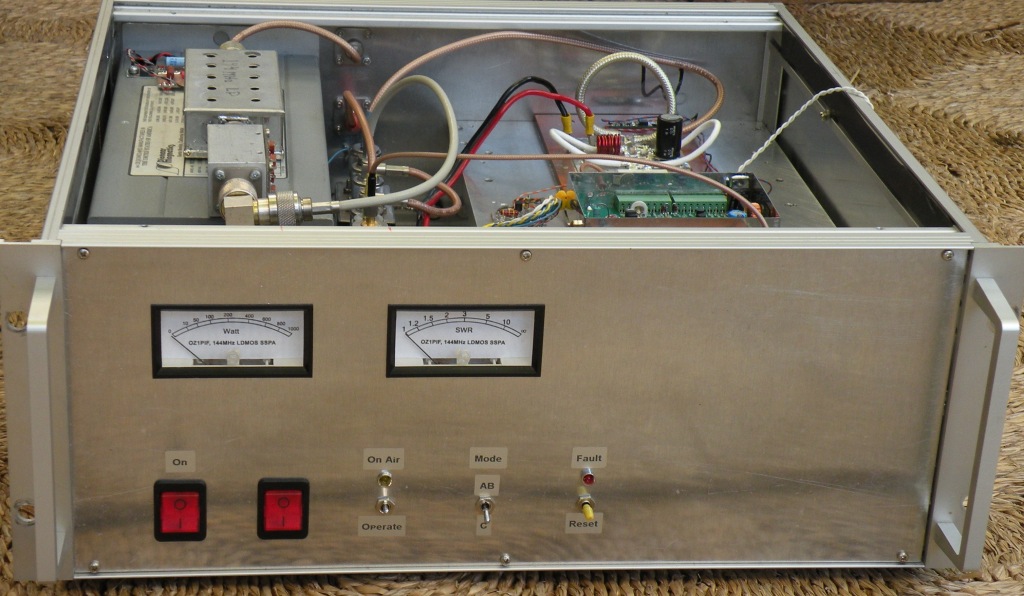
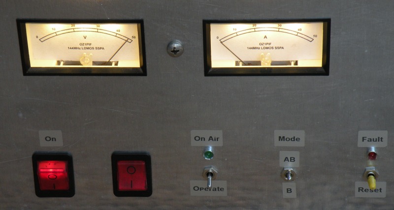
And finally from the front with operational controls and indicators.
12.07.2011:
Last night it was time for the initial smoke-test. The first power-up
(current limited power supply) went fine with no signs of oscillations
or other untoward phenomenons. After a few attempts to adjust the gate
bias correctly I noticed the silk-screened "(first)" next to the mode
"B" adjustment (no mentioning of this in the documentation), and from
then on adjustment proceeded smoothly.
Time had come to move the RF-module to the internal high-current power
supply! Also no problem, but then - as more power was fed to the
amplifier - a loud noise, followed by bright arc'ing from C19/C20
happened - ouch! These were two of the caps I relocated after being
told that they were less than optimally mounted, one blew and the other
was badly singed. It may certainly be the case that it was damaged
during the unsolder/re-solder process, and that this was the cause of
the failure.
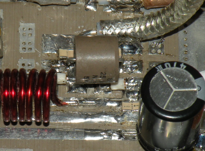
No direct replacement was at hand, but a 25pF/5KV high-power cap was
found as a stop-gap replacement, and testing could continue, although
some of the results may be less than valid because of the lower
capacitance installed. Please bear this in mind as you read on.
As power out approached 1KW, three things were noticed: a) efficiency
was low, b) more than 5W input was required to get 1KW out, and c)
power out reading on the attached Bird Power Meter was low compared to
what was measurable when taken before the LP filter to an HP Power
Meter. When checked on a spectrum analyser a significant harmonic
content (not present in the input) was noticed, 3'rd harmonic in
particular was only 10-12dB down from the carrier level.
This part of testing is inconclusive however because of the 25pF
substitution for 30pF, and will have to be repeated once replacement
caps have been acquired (either 2 x 15pF as originally supplied or 3 x
10pF for a higher current capability).
Here's the temporary C19/C20 25pF/5KV replacement cap:
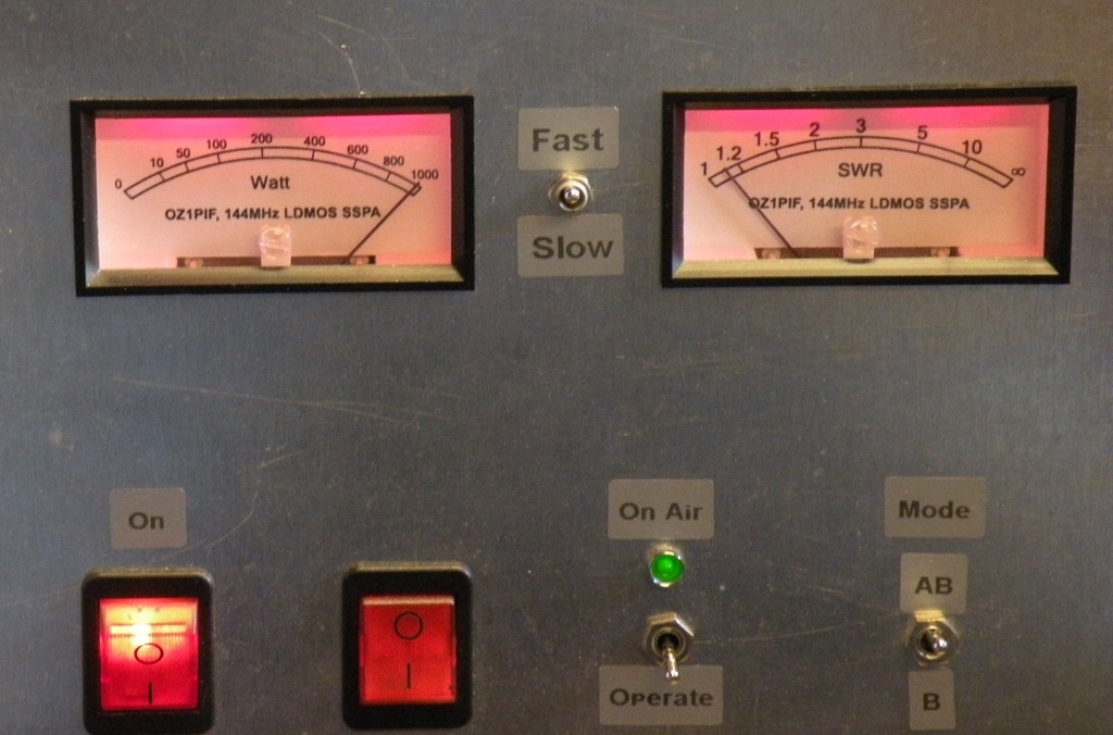
24.07.2011: Meanwhile I'm debugging my SWR-Computer/Power-meter, here 45W into a 1:1 (50 Ohm) load:
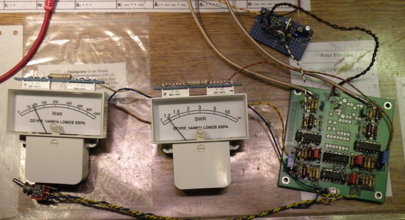
The attachments on top of the instruments are are four quad LED arrays
serving as instrument illumination (Red light!, but that's all I had
available), when finished a comparator (separate PCB) will
trip the PA control-module when SWR gets to high. The switch in the
foreground is for selecting fast/slow decay. The SWR instrument will
not show a 1:1 since the directivity of the coupler used is far from
optimal (only some 28dB), as soon as the return loss gets worse than
that, the instrument shows a correct value regardless of whether power-out is 10
or 1000W.
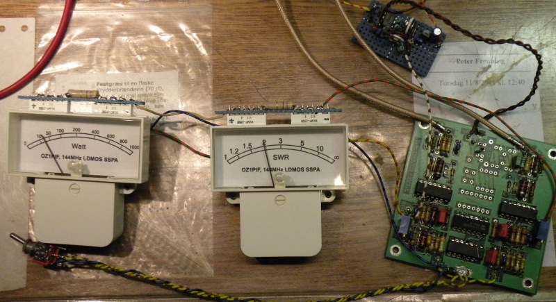
Seen here 45W into a 25 Ohm load (tranceiver reduces output to some 20W because of the mismatch):
20.08.2011: Last night the
whole project reached a longed for milestone - it became an operational
amplifier! albeit with a couple of items missing or in need
of improvement:
The Drain voltage sags some 4V at full song.
Some issues with the SWR display still needs to be resolved.
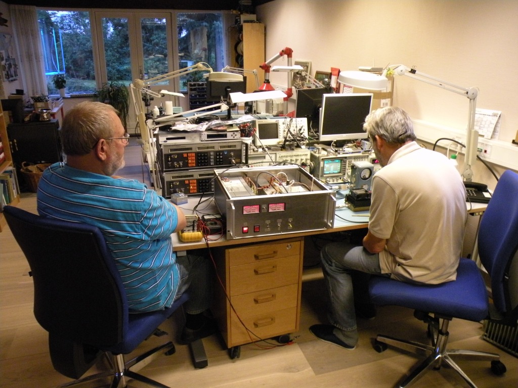
OZ7YK, Kurt and OZ3SW, Steen studying the output during the test-session at OZ3SW's lab.
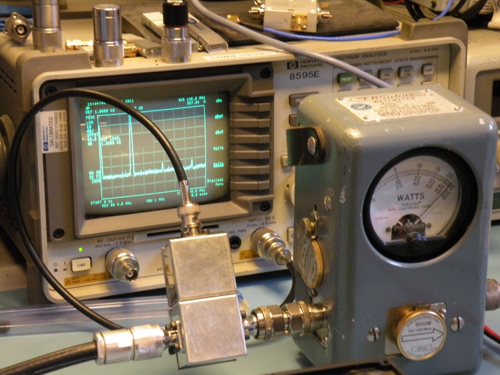
867W out with 2'nd and 3'rd harmonics below -50dB (after LP-filter).
Nearly 1KW out, here shown on on-board instrumentation (Peak Watt-meter)
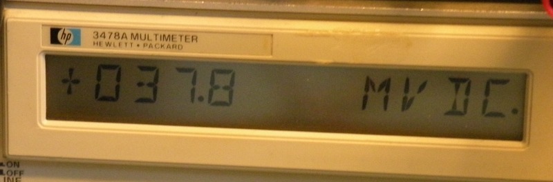
Using 37.8A (measured over 0.001Ohm shunt just prior to the RF-module), 44V supply at Drain, amp running just over 1KW at 4.7W input.
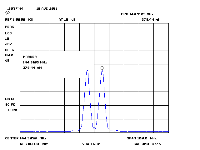
Signal from two-tone generator.
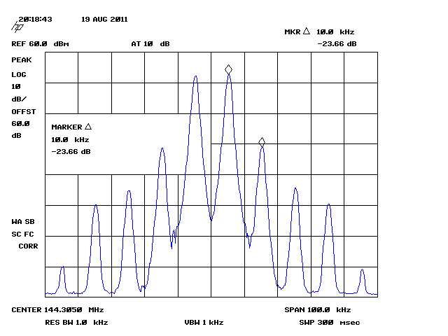
IMD at 730W PEP
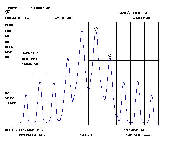
IMD at 900W PEP
The IMD results are somewhat disappointing, I would have liked to see figures 5-10dB better, as it is I'll probably limit power out for SSB usage to 900W.
Efficiency is also below expected values, partially due to the voltage sag, and will probably increase when I solve that.
A quick on-the-air test late last night yielded positive reports of "a clean strong signal" a station reported being able to hear my "splatter" only some 5-6KHz to either side despite copying my signat at S9+
The thermal behaviour of the amplifier seems to be excellent, it being able to absorb 2-minute at full output without any undue heat problems, after several such periods the "hot-fans" kick in (at 45॰C heat-sink temp) and takes care of business.
One very nice thing about a SSPA is how quiet it is in the shack with it running, compared to what I had to contend with from my Gi7b amp.
21.08.2011: One problem has cropped up though - when transmitting, the voltage from the SMPS fluctuates with the amount of RF generated, most noticeably with the lid on the amplifier (which is why it wasn't noticed during lab-testing), signifying that it is probably stray RF being picked up by the wiring to the SMPS....
This may also be behind some of the other problems noted.
21.08.2011 Update: A liberal application of clip-on ferrites seems to have mostly cured this symptom.
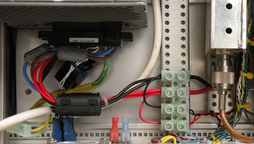
Ferrites clipped on to all leads to/from the SMPS.
Power leads to the RF-module, also seen in this shot: the 0.001 Ohm shunt for measuring current used by the RF-module.
03.10.2011: Today it finally happened, after more than 50 hours of full, or nearly full, power output, a loud "plop" was heard from the amp, followed by an ugly "burnt smell". As luck will have it, it turned out to be caused by a total failure of the output coax-relay:
This is what the post-mortem revealed!!!!!
As luck would also have it, it seems that the amplifier device is robust enough to have survived the infinite SWR resulting (open), despite my lack of SWR protection (yet to be implemented).
Now I'm trying to decide how to progress, as I see it I have three options: 1) Buy a new and heftier relay; 2) use some form of Pin-diode switch instead; or 3) To eliminate Tx-Rx switching altogether (I'm running separate Tx Rx coaxes anyway).
In the interim I'm running the amp with no internal Rx-Tx switching, inserted in the (separate) Tx coax-line, and it's been running like this for almost 2 hours with no indication of problems.
This what a close-up reveals after some cleaning:
Both contact reeds have partially evaporated/melted, leaving part of the melted material on the center pin. The right hand (output side) plexiglass push-rod is almost entirely gone.
24.03.2013 Several things have been modified lately:
Much thicker wiring for 50V DC to amplifier module;
Transceive capability restored with new coax-relays: Tohtsu CX-600N and CX520D (12V coils);
High power signal routing now made with RG214 and RG393 10mm coax;
New fan in power supply (the original was too noisy);
Directional coupler, -50dB/34dB directivity now inserted in circuit;
Instruments now display V and A and have new white LED-illumination:
Things still outstanding (until I dream up even more):
Improved thermostatic fan control;
Digital Power-Out/SWR display;
High-SWR sense and signaling to controller;
Remote voltage sense implementation;
LP-filter before amplifier (why waste power on amplifying 3'rd harmonic content from driver);
After the general clean-up and rewiring, it would seem to have increased output some 10-15% and efficiency to around 66%.
Real hard numbers will have to wait until I can get it to the lab for proper testing, I'm also very interested in seeing current IMD figures!